SUN STUFF INJURY ATTORNEYS
WHAT WE DO
Investigation
Legal Expertise
Negotiations
Client Advocacy
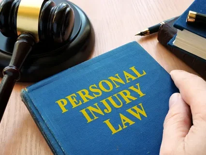
Understanding the Role of Personal Injury Lawyers: A Comprehensive Guide by Sun Stuff Injury Attorneys
Navigating the aftermath of a personal injury requires not only resilience but also the expertise of seasoned legal professionals. In the intricate realm of personal injury law, the role of attorneys becomes paramount. This comprehensive guide aims to shed light on the multifaceted responsibilities and significance of personal injury lawyers, with a particular emphasis on the exemplary services provided by Bronx Injury Lawyers P.C.
1. Legal Expertise and Case Evaluation:
At the core of a personal injury attorneys role lies a profound understanding of the legal landscape. Sun Stuff Injury Attorneys, with their wealth of experience, conduct a meticulous case evaluation to assess the merits of each case comprehensively. This involves a detailed analysis of the circumstances surrounding the injury, enabling the formulation of a tailored legal strategy.
2. Compassionate Client Support:
Beyond the legal intricacies, personal injury lawyers from Sun Stuff Injury Attorneys understand the emotional and physical toll that injuries can inflict on individuals and their families. Their role extends to providing compassionate support, offering guidance through the legal process, and addressing the broader impact of the incident on the client's life.
3. Thorough Investigation and Evidence Gathering:
Building a compelling case requires a thorough investigation and the gathering of substantive evidence. Sun Stuff Injury Attorneys employ a meticulous approach, collaborating with experts such as accident reconstruction specialists, medical professionals, and forensic analysts. This commitment ensures that the evidence presented is robust, enhancing the chances of a favorable outcome for the client.
4. Legal Representation in Negotiations:
A significant portion of a personal injury lawyer's role involves negotiating on behalf of the client. Sun Stuff Injury Attorneys are adept negotiators, striving to secure fair compensation for their clients to cover medical expenses, lost wages, and other damages resulting from the personal injury. Their focus is on achieving a resolution that is just and comprehensive.

5. Litigation and Courtroom Advocacy:
While many personal injury cases are resolved through negotiations, some may proceed to litigation. In such instances, the personal injury lawyers role evolves into that of a courtroom advocate. Sun Stuff Injury Attorneys exhibit seasoned litigation expertise, presenting compelling arguments and evidence before a court to secure a favorable outcome for their clients.
6. Determining Fault and Liability:
Establishing fault and liability is a critical aspect of personal injury cases. Sun Stuff Injury Attorneys employ a meticulous approach to analyze the circumstances of the incident, identify responsible parties, and build a persuasive case. This determination is crucial for pursuing a successful claim and ensuring that the client receives just compensation.
7. Communication with Insurance Companies:
Navigating the intricacies of dealing with insurance companies is a key responsibility of a car accident attorney. Sun Stuff Injury Attorneys serve as effective liaisons, communicating with insurance adjusters on behalf of their clients. This ensures that the client's rights are protected, and negotiations are conducted with a focus on achieving a fair settlement.
8. Determination of Damages and Compensation:
Part of the personal injury lawyer's responsibility involves determining the extent of damages suffered by the client. This includes financial losses, such as medical expenses and lost income, as well as non-economic damages like pain and suffering. Sun Stuff Injury Attorneys ensure a comprehensive assessment, seeking compensation that reflects the full impact of the personal injury.
Curious if you have a personal injury case? Visit www.nyc-injury-attorneys.com for a free consultation.
In conclusion, understanding the role of personal injury lawyers involves recognizing the intersection of legal expertise, strategic planning, and compassionate advocacy. Sun Stuff Injury Attorneys stands as a paragon of legal excellence, offering a comprehensive guide for individuals navigating the challenges associated with personal injury incidents. Their attorneys are dedicated to upholding justice and securing the best possible outcomes for their clients in the complex landscape of personal injury law.
OUR CLIENT REVIEWS
Their attention to detail in building my case was impressive, and I could sense their dedication to securing the best outcome. I highly recommend the services of a personal injury lawyer to anyone in need of professional legal representation.

Gary M. Birt
The lawyer's commitment to thorough investigation and meticulous case preparation was evident throughout. What stood out to me was their effective communication – keeping me informed and engaged in the process.
William L. McCoy
CONTACT US
Your Shield in Times of Crisis- A Spotlight on the Best Personal Injury Lawyers
In the realm of unforeseen accidents and life-altering events, the role of a personal injury lawyer becomes paramount. These legal professionals, often unsung heroes in the pursuit of justice, serve as shields for individuals facing crises arising from injuries. In this spotlight on the best personal injury lawyers...
Copyright 2018 | SUN STUFF INJURY ATTORNEYS
| All Rights Reserved